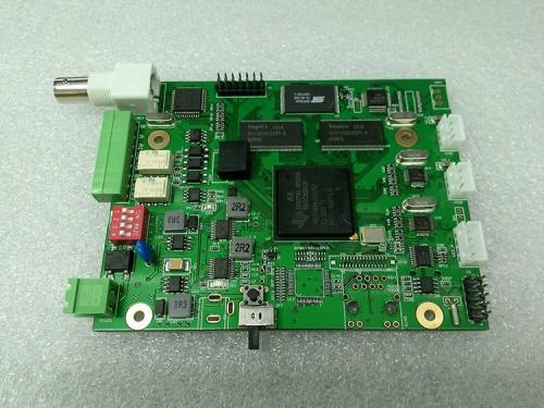
BGA for SMT chip processing is a kind of packaging method. BGA is the abbreviation of ball grid array, which translates into ball grid array packaging in Chinese. In the 1990s, with the continuous development of electronic technology, the processing speed of IC is also continuously improving. With the continuous improvement of the number of I / O pins on the IC chip, the elements at all levels clearly put forward higher requirements for IC packaging. In addition, in order to consider the development of electronic equipment towards miniaturization and precision, BGA packaging is coming out and put into production. Next technology professional SMT SMT chip processing plant pater high precision to introduce the basic BGA processing information content.
1、 Steel mesh
The thickness of steel mesh is generally 0 in SMT chip processing, but in the welding process of BGA devices, the thick steel mesh is likely to lead to tin bonding. According to Pater's high-precision surface assembly production experience, the thickness of steel mesh is very suitable for BGA devices, and it can also moderately expand the total area of steel mesh opening.
2、 Solder paste
BGA devices have small spacing between pins, so the solder paste used also requires small particles of metal materials. Too large particles of metal materials will cause tin bonding in SMT processing.
3、 Welding temperature setting
In the whole process of SMT chip processing, reflow soldering furnace is generally used. Before welding BGA package components, the temperature of each area must be set according to the processing regulations, and the temperature around the spot welding must be detected by thermal resistance camera.
4、 Inspection after welding
After SMT processing, it is necessary to carry out strict detection on BGA packaged devices, so as to prevent some chip defects.
5、 Advantages of BGA package:
1. The rate of finished products increased;
2. The electric heating performance is improved;
3. The volume and mass decrease;
4. The parasitic parameters decreased;
5. The signal transmission delay is small;
6. The use frequency is increased;
7. The credibility of commodities is high;
6、 Defects of BGA package:
1. The inspection after welding must be based on X-ray;
2. The cost of electronic production increased;
3. The cost of repair increases;
Because of its packaging characteristics, BGA has a great difficulty in SMT chip welding, and casting defects and repair are also difficult to operate in practice, so as to ensure the welding quality of BGA devices. SMT chip manufacturers generally pay attention to the customization of processing regulations from the following aspects.
