PCB design flow of RF circuit
Because Protel99SE software is different from Protel 98, this paper first discusses the PCB design process by Protel99SE software.
Because Protel99SE adopts engineering database mode management, it is implicit in Windows 99, so a database file should be established to manage circuit schematic diagram and PCB layout.
(2) In order to realize network connection, the components used in the principle design must exist in the component library, otherwise the components needed must coexist in the storage file of schlib, and then only call the required components from the component library and connect according to the designed circuit diagram.
(3) After the design of the schematic, the network table can be formed for PCB design.
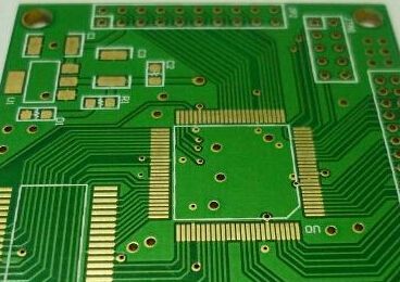
Design of 4pcb
Determination of PCB shape and size. According to the position of PCB, the size and shape of space and the cooperation with other parts, the shape and size of PCB are determined. The shape of the PCB is drawn by the placetrack command of the mechicallayer layer.
b. According to the requirements of SMT, make positioning holes, eyes, reference points, etc. on PCB.
c. Manufacturing of components. If you need to use some special components that do not exist in the component library, you need to generate the components before you layout. The process of making Protel99SE component is relatively simple. After selecting the makelibrary command in the design menu, enter the component creation window, and then you can select the newcomponent command on the tool menu to design the component. At this time, only draw the corresponding pad according to the shape and size of the actual component in the toplayer layer, and edit it into the required pad (including the shape, size, inner diameter and angle of the pad, and the corresponding pin name of the pad). In addition, the corresponding pad pin name should be marked, Then use the placetrack command to draw the maximum shape of the component at the topoverlay layer and store the component name in the component library.
After the component is finished, layout and wiring are carried out, and the two parts are discussed in detail below.
(the network formed by the schematic diagram can be compared with the network formed by PCB) it must be checked after the above process is completed. On the one hand, it includes the inspection of circuit principle, on the other hand, it also needs to check the matching and assembly problems between each other. The circuit principle can be checked manually or automatically by the network (the network composed of the schematic can be compared with the network formed by PCB).
f. After the check, the file is archived and output. In Protel99SE, you must use the export command in the file option to store the file in the specified path and file (the Import command is to transfer a file to Protel99SE). Note: in the file option in Protel99SE, "savecopyas." After executing the command, the selected file name is not visible in Windows 98, so the file is not visible in Explorer. This is similar to the "file" in PROTEL98. The function is not exactly the same.
